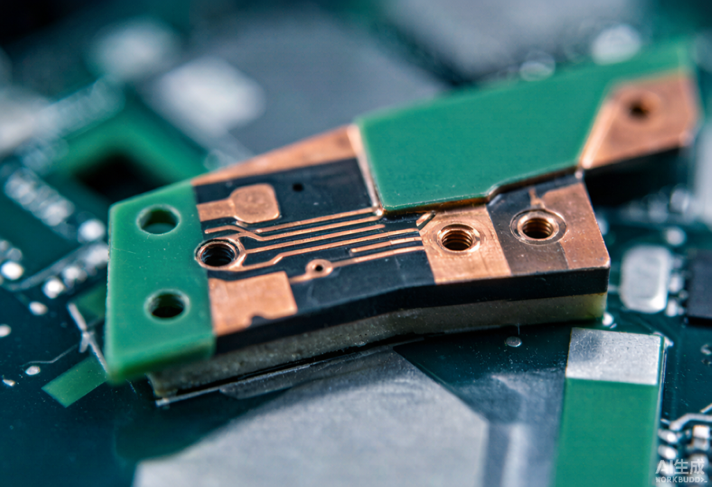
Beyond Opens and Shorts: The Hidden Defect Spectrum in High-Precision PCBs
Most engineers are familiar with opens and shorts — the two most common electrical defects in PCB manufacturing. But in high-precision applications, these defects manifest in far more insidious forms: a line width that narrows to 50% of design value, a wedge-shaped gap invisible to the naked eye, a thin film of residual copper that passes AOI but causes leakage current in the field.
At Leyi Trading, we’ve spent 20 years manufacturing multilayer, HDI, and high-frequency PCBs. This article maps eight typical defects across four core processes — pattern transfer, electroplating, lamination, and surface finish — covering their microscopic morphology, causal mechanisms, and engineering impact. The goal: equip design engineers and procurement professionals with a sharper analytical framework for interpreting supplier inspection reports.
1. Pattern Transfer Defects: When Opens and Shorts Evolve
Opens and shorts are the most common electrical defects in PCBs, but in high-precision applications they manifest in more variant forms — and detection difficulty rises correspondingly.
Micro-open
A micro-open is not a complete line break, but a local reduction of line width below 50% of the design value. In AOI images it appears as “necking” — uneven exposure energy or developer temperature fluctuations cause the dry film to develop with wavy edges, and the thinnest points are over-etched during subsequent processing.
Micro-opens often still pass flying probe testing (because the residual copper remains continuous), but under high current or high-frequency signals they become hotspots and reflection points, compromising long-term reliability. This makes them one of the most dangerous defect types — invisible to electrical testing, yet catastrophic in the field.
Residual Copper Short
Particularly problematic in fine-pitch areas. During etching, if spray pressure is insufficient or copper ion concentration is too high, extremely thin copper residue (often less than 5µm) remains in non-conductive regions between traces. This residual copper has low optical contrast and is easily missed by automated inspection, yet it is sufficient to cause leakage current exceedance between adjacent signal lines — with disproportionate impact on high-impedance circuits.
2. Electroplating Defects: Hole-Wall Cracks and Surface Nodules
For multilayer boards, via reliability directly determines product lifetime. Cross-section analysis during PCB prototyping frequently reveals two categories of plating defects that are invisible from the surface but devastating in performance.
Wedge Void
Manifests as a wedge-shaped gap between the plating layer and the inner-layer copper ring. The root cause is that glass fiber bundles torn during drilling are not fully removed, and the desmearing process fails to clean the area thoroughly. As a result, no copper layer adheres during electroless copper deposition, and the plating cannot form a metallurgical bond with the inner copper ring.
This defect deteriorates rapidly under thermal shock testing and is a major hidden risk for multilayer board reliability — often surviving initial QC only to fail during field thermal cycling.
Nodule
Refers to spherical copper lumps appearing at via openings or surface trace corners. They originate from additive imbalance in the plating bath (excess brightener or insufficient leveler), causing abnormal local current density. Beyond cosmetic concerns, copper nodules can pierce adjacent prepreg during lamination, reducing interlayer insulation thickness and triggering dielectric breakdown failures.
3. Lamination and Dielectric Defects: Voids and Fiber Shift
Defects introduced during lamination are typically “non-repairable” — once internal layers are sealed, intervention is impossible. Prevention is therefore far more valuable than detection.
Interlayer Void
The most common lamination defect, appearing as transparent circular cavities in the prepreg under microscopic cross-section. Causes include:
- Moisture absorbed by prepreg that was not adequately baked (vaporizing at high temperature)
- Excessive lamination heating rates that trap air behind the resin flow front
- Excessive inner-layer copper area impeding uniform resin fill
Voids significantly reduce dielectric strength and are prone to cause breakdown during hipot testing — making them a critical failure mode in high-voltage PCB applications.
Fiber Shift
Occurs under high pressure when the glass fiber cloth in the prepreg is displaced, resulting in uneven fiber density distribution in the dielectric layer. This affects differential pair signal phase consistency and is particularly fatal for serial links above 10Gbps — signal integrity issues often only surface at system-level testing, making root-cause tracing extremely costly.
4. Surface Finish Defects: Nickel Corrosion and White Gold
Surface finish is the final process gate before a PCB reaches the assembly line. Two defects here directly impact solderability and joint reliability.
Nickel Corrosion (“Black Nickel”)
Appears as black spots or gray bands at pad edges. The root cause is excessive attack on the nickel layer by gold ions during the immersion gold displacement reaction. When corrosion depth exceeds 3µm, solderability drops sharply and false soldering occurs during SMT assembly — making it the primary factor affecting solder joint yield in the surface finish process.
White Gold
Typically refers to insufficient electroless gold thickness (below 0.03µm) or uneven deposition, exposing the underlying nickel color. This is easily flagged as non-conforming during visual inspection and requires verification of the supplier’s gold thickness control standards and batch inspection data.
The Engineering Logic: Defects Don’t Occur in Isolation
It is worth noting that most of the above defects do not occur in isolation. Etching non-uniformity typically couples with copper foil thickness deviation and etchant temperature gradients; plating nodules strongly correlate with anode life and additive replenishment cycles for the production batch. Detecting defects is not the hard part — AOI and microscopy already cover most scenarios. The real value lies in mapping defect morphology to specific process parameters.
For example:
- A particular notch morphology points to excessive exposure energy
- A particular residual copper pattern points to delayed etchant replenishment
- A particular wedge void shape points to low desmearing temperature
For design engineers, proactively understanding these defect signatures during the prototyping stage not only aids in interpreting supplier inspection reports but also enables targeted redundant design in subsequent revisions — such as widening specific net traces or adding test pads — striking a better balance between design intent and manufacturing reality.
Typical defects in high-precision PCBs are fundamentally the product of the interplay between physical limits, chemical controllability, and pattern complexity. From the “necking” of micro-opens to the “wedge gap” of hole-wall separation, from interlayer voids to nickel corrosion, each defect carries a unique microscopic fingerprint and process attribution. The key to defect management is not eliminating all defects, but maintaining a clear understanding of each defect’s causal boundaries — and making rational trade-offs between cost and reliability.
Partner With a Manufacturer That Understands Defect Management
At Leyi Trading, we don’t just detect defects — we trace them to their root causes. With over 20 years of PCB manufacturing experience, ISO 9001 and IATF 16949 certifications, and a factory expanding to 3x capacity in 2026, we deliver the quality and reliability your projects demand.
Our engineering team provides DFM feedback that goes beyond simple pass/fail — we help you understand why a defect occurred and how to prevent it in your next revision. Whether you need impedance-controlled boards for 5G infrastructure, high-layer-count boards for AI accelerators, or rugged PCBs for industrial automation, our defect management expertise ensures your design performs as intended.
Ready to discuss your PCB project? Get a quote within 24 hours — our engineering team will review your design and provide DFM feedback at no cost.